绘制中学物理电路图
Table of Contents
1. TiKZ 与中学数理
北师大物理系毕业的同学,经历漫长的耕耘,穿越黑铁、青铜、白银,终于进入了黄金时代——厚重而闪耀,重剑无锋,明媚而干净,让人不由心生羡慕。
这些年来,我知道了:
- TiKZ 几件事
- TiKZ 适合物理、数学教材的插图,
- TiKZ 在 \( \LaTeX{} \) 里使用更方便,
- TiKZ 在 Org Mode 里画图不是很方便。
- \( \LaTeX \) 几件事
- 最方便安装使用的 \( \LaTeX{} \) 环境是 Tectonic,用 Rust 开发,
- Tectonic 有现代的 \( \TeX \) 包管理,这是它真正区别于其他 \( \LaTeX{} \) 环境的地方。
- TiKZ 编译要用 \( \LaTeX{} \) 环境,比如 Tectonic。
- Org Mode 几件事
- Org Mode 写文档比 \( \LaTeX{} \) 、Markdown 以及 Word 都方便,
- Org Mode 使用 Org Babel 生成图片,比如 plantuml, d2, mermaid 等,
- Org Mode 可以导出为 Markdown, html, \( \LaTeX{} \) , PDF 等格式。
我给 slingshot1 增加了子命令 tikz :
slingshot tikz input.tikz output.png # png 格式
slingshot tikz input.tikz output.svg # svg 格式
slingshot tikz input.tikz output.pdf # pdf 格式
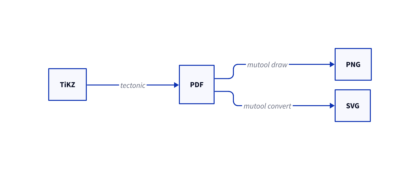
Figure 1: Slingshot TiKZ 架构
在 ob-tikz2 项目里增加了 ob-tikz.el 和 tikz-mode.el 两个包。为方便使用,在 tikz-mode.el 里实现了图片预览功能。我被 AI 惯坏了,代码习惯性地转给 dscli3 写。
本文档除介绍中学物理电路图 CircuiTikZ 的画法外,还用来测试 slingshot
tikz 画电路图。 slingshot tikz 省去 tectonic 编译 TiKZ 的繁琐,提供易用性,同时要保证高大上的 TiKZ 满足中学物理数学的实际需要。
生物电测量前端:皮肤电极(Body)拾取的差分信号 v+、v−经高通滤波进入仪表放大器 LNA(AD8429),E+、E−、Egnd 为电极偏置电源;四个开关(ADG1414)由微控制器(μC)经 ADC 数字控制,虚线框分别标出人体、电极、接地电极与开关组的区域。
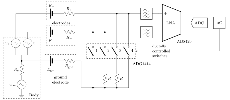
Figure 2: 一种风格低噪音输入级
\begin{circuitikz}[scale=1.4]
  \draw (0,0) to[C, l=10<\micro\farad>] (0,2) -- (0,3)
        to[R, l=2.2<\kilo\ohm>] (4,3) -- (4,2)
        to[L, l=12<\milli\henry>, i=$i_1$,v=b] (4,0) -- (0,0)
  (4,2) to[D*, color=red] (2,0)
  (0,2) to[R, l=1<\kilo\ohm>, *-] (2,2)
        to[cV, i=1, -*, v=$\SI{.3}{\kilo\ohm}\, i_1$] (4,2)
  (2,0) to[I, i=1<\milli\ampere>, *-*] (2,2);
\end{circuitikz}
回路串联 10 μF 电容、2.2 kΩ电阻与 12 mH 电感(电流 i₁),红色发光二极管接在电阻与电感之间;另一支路由 1 kΩ电阻、受控电压源(0.3 kΩ·i₁)和 1 mA 电流源组成。
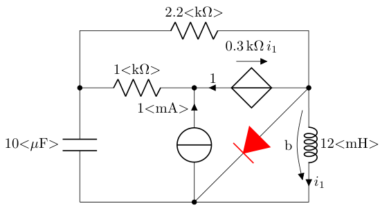
Figure 3: A red diode
%% Using the (experimental) siunitx syntax
\begin{circuitikz}[scale=1.2]
  \draw (0,0) node[ground] {}
  to[V=$e(t)$, *-*] (0,2) to[C=4<\nano\farad>] (2,2)
  to[R, l_=.25<\kilo\ohm>, *-*] (2,0)
  (2,2) to[R=1<\kilo\ohm>] (4,2)
  to[C, l_=2<\nano\farad>, *-*] (4,0)
  (5,0) to[I, i_=$a(t)$, -*] (5,2) -- (4,2)
  (0,0) -- (5,0)
  (0,2) -- (0,3) to[L, l=2<\milli\henry>] (5,3) -- (5,2)
  {[anchor=south east] (0,2) node {1} (2,2) node {2} (4,2) node {3}};
\end{circuitikz}
电压源 e(t) 与 4 nF 电容、0.25 kΩ电阻构成第一节,1 kΩ电阻与 2 nF 电容构成第二节,电流源 a(t) 从右侧注入,上方 2 mH 电感横跨输入输出两端;节点 1、2、3 依次标注。
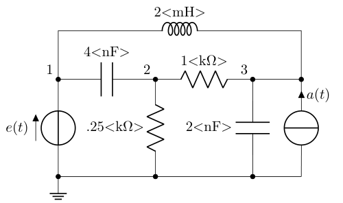
Figure 4: 使用(实验性)siunitx 语法
%% Using the (experimental) siunitx syntax
\begin{circuitikz}[scale=1.2]\draw
  (0,0) node[anchor=east] {B}
        to[short, o-*] (1,0)
        to[R=20<\ohm>, *-*] (1,2)
        to[R=10<\ohm>, v=$v_x$] (3,2) -- (4,2)
        to[cI=$\frac{\si{\siemens}}{5} v_x$, *-*] (4,0) -- (3,0)
        to[R=5<\ohm>, *-*] (3,2)
  (3,0) -- (1,0)
  (1,2) to[short, -o] (0,2) node[anchor=east]{A}
;\end{circuitikz}
二端口网络:上端 A、下端 B 为两个端口。B 端经 20 Ω电阻、10 Ω电阻(电压 v_x)串联到节点,受控电流源(v_x/5 S)与 5 Ω电阻并联在节点与底轨之间, A 端从两电阻中点引出。
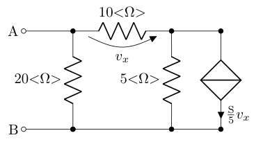
Figure 5: Using the (experimental) siunitx syntax
\begin{circuitikz}[scale=1]\draw
   (0,0) node[transformer] (T) {}
   (T.B2) to[pD] ($(T.B2)+(2,0)$) -| (3.5, -1)
   (T.B1) to[pD] ($(T.B1)+(2,0)$) -| (3.5, -1)
;\end{circuitikz}
变压器副边的两个输出端各接一个光电二极管(pD),汇合到一点。
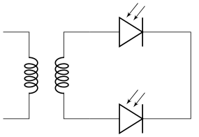
Figure 6: 光电二极管
\begin{circuitikz}[scale=1.2, american]\draw
  (0,2) to[I=1<\milli\ampere>] (2,2)
        to[R, l_=2<\kilo\ohm>, *-*] (0,0)
        to[R, l_=2<\kilo\ohm>] (2,0)
        to[V, v_=2<\volt>] (2,2)
        to[cspst, l=$t_0$] (4,2) -- (4,1.5)
        to [generic, i=$i_1$, v=$v_1$] (4,-.5)
        -- (4,-1.5)
  (0,2) -- (0,-1.5) to[V, v_=4<\volt>] (2,-1.5)
        to [R, l=1<\kilo\ohm>] (4,-1.5);

   \begin{scope}[xshift=6.5cm, yshift=.5cm]
     \draw [->] (-2,0) -- (2.5,0)
     node[anchor=west] {$v_1/\si{\volt}$};
     \draw [->] (0,-2) -- (0,2)
     node[anchor=west] {$i_1/\si{\milli\ampere}$} ;
     \draw (-1,0) node[anchor=north] {-2} (1,0)
     node[anchor=south] {2} (0,1)
     node[anchor=west] {4} (0,-1)
     node[anchor=east] {-4}
          (2,0) node[anchor=north west] {4}
          (-1.5,0) node[anchor=south east] {-3};
     \draw [thick] (-2,-1) -- (-1,1)
     -- (1,-1) -- (2,0) -- (2.5,.5);
    \draw [dotted] (-1,1) -- (-1,0) (1,-1) -- (1,0)
          (-1,1) -- (0,1) (1,-1) -- (0,-1);
   \end{scope}
\end{circuitikz}
左侧电路含 1 mA 电流源、2 V 电压源、开关 t₀及待测元件(i₁、v₁),右侧画出该元件的 v₁–i₁伏安特性曲线。
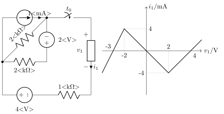
Figure 7: Mixing circuits and graphs
\begin{circuitikz}[scale=1]
    \ctikzset{bipoles/detector/width=.35}
    \ctikzset{quadpoles/coupler/width=1}
    \ctikzset{quadpoles/coupler/height=1}
    \ctikzset{tripoles/wilkinson/width=1}
    \ctikzset{tripoles/wilkinson/height=1}
    %% \draw[help lines,red,thin,dotted] (-5,-5) grid (5,5);
    \draw
    (-2,0) node[wilkinson](w1){}
    (2,0) node[coupler] (c1) {}
    (0,2) node[coupler,rotate=90] (c2) {}
    (0,-2) node[coupler,rotate=90] (c3) {}
    (w1.out1) .. controls ++(0.8,0)
    and ++(0,0.8) .. (c3.port3)
    (w1.out2) .. controls ++(0.8,0)
    and ++(0,-0.8) .. (c2.port4)
    (c1.port1) .. controls ++(-0.8,0)
    and ++(0,0.8) .. (c3.port2)
    (c1.port4) .. controls ++(-0.8,0)
    and ++(0,-0.8) .. (c2.port1)
    (w1.in) to[short,-o] ++(-1,0)
    (w1.in) node[left=30] {LO}
    (c1.port2) node[match,yscale=1] {}
    (c1.port3) to[short,-o] ++(1,0)
    (c1.port3) node[right=30] {RF}
    (c2.port3) to[detector,-o] ++(0,1.5)
    (c2.port2) to[detector,-o] ++(0,1.5)
    (c3.port1) to[detector,-o] ++(0,-1.5)
    (c3.port4) to[detector,-o] ++(0,-1.5)
    ;
\end{circuitikz}
射频测量前端:本振 LO 经威尔金森功分器(Wilkinson)分成两路,RF 信号从耦合器 c1 输入(port2 接匹配负载);两路信号经 90°耦合器 c2、c3 交叉分配,最后由四个检波器(detector)输出。
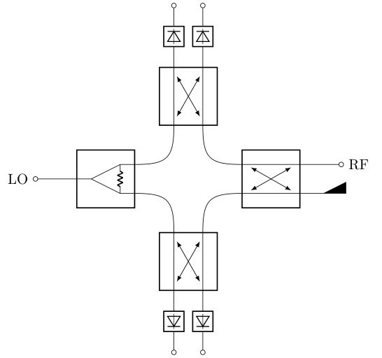
Figure 8: 射频电路(RF circuit)
\begin{circuitikz}[scale=1]\draw
    (5,.5) node [op amp] (opamp) {}
  (0,0) node [left] {$U_{we}$}
  to [R, l=$R_d$, o-*] (2,0)
    to [R, l=$R_d$, *-*] (opamp.+)
    to [C, l_=$C_{d2}$, *-] ($(opamp.+)+(0,-2)$)
    node [ground] {}
    (opamp.out) |- (3.5,2)
    to [C, l_=$C_{d1}$, *-] (2,2)
    to [short] (2,0)
    (opamp.-) -| (3.5,2)
    (opamp.out)
    to [short, *-o] (7,.5)
    node [right] {$U_{wy}$}
;\end{circuitikz}
Sallen-Key 二阶低通滤波单元:输入 U_we 经两个等值电阻 R_d 送入运放同相端, C_d2 在同相端接地,运放输出经 C_d1 反馈至两电阻中点,输出 U_wy。
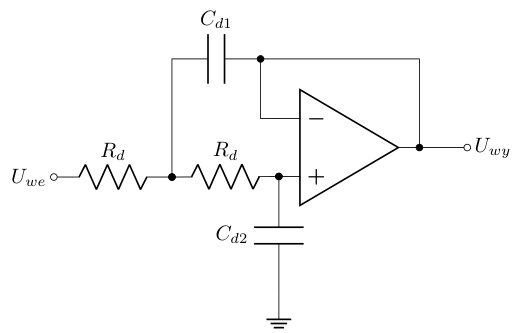
Figure 9: A Sallen-Key cell
\begin{tikzpicture}[circuit ee IEC]
 \draw (0,0) to [resistor={name=R}] (0,2)
  to[diode={name=D}] (3,2);
  \draw (0,0) to[*R=$R_1$] (1.5,0)
  to[*Tnpn] (3,0)
   to[*D](3,2);
\end{tikzpicture}
circuit ee IEC 兼容模式示例:上方支路为电阻 R 与二极管 D 串联,下方支路为电阻 R₁、NPN 三极管与二极管相连。
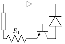
Figure 10: 兼容模式的一个例子
三相输变电示意图:左侧电网经 Y/Δ变压器进入 AC/DC 换流器,红色开关处标注 fault(故障);直流线路(HVDC line)传输后经 DC/AC 换流器变回交流,再由Δ/Δ/Y 变压器接入右侧电网。

Figure 11: 三相块示意图(3-phases block schematic)
2. 点亮小灯泡
\begin{circuitikz}
  \draw (0, 0) to[battery1] (4,0)
  -- (4,2) to[lamp=L] (2,2);
  \draw (0,0) -- (0,2)
  to[nos,a=S] (2,2);
\end{circuitikz}
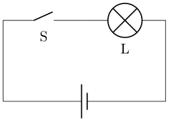
Figure 12: 点亮小灯泡
在画电路图时请注意:
- 使用统一规定的符号,
- 尽量避免连线交叉,
- 连线要横平竖直,尽量使电路图简洁美观。
3. 常见元器件
\begin{circuitikz}
  \draw (0,0) to[lamp, a=灯泡] (0,2);
  \draw (3,0) to[battery1, a=电池] (3,2);
  \draw (0,3) to[buzzer, a=电铃] (0,5);
  \draw (3,3) to[nos, a=开关] (3,5);
  \draw (0,6) to[motor,l=电动机] (3,6);
  \draw (1.5,-0.8) node[spdt] (S) {};
  \draw (1.5,-2.1) node[above]{单刀双掷开关};
  \draw (S.out 1) node[right]{out 1};
  \draw (S.out 2) node[right]{out 2};
  \draw (S.in) node[left]{in};
\end{circuitikz}
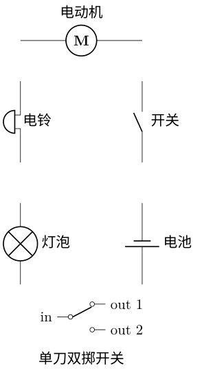
Figure 13: 常见元器件:灯泡、电池、电铃、开关、电动机等
CircuiTikZ 宏包还提供了各种各样的元器件,这些元器件都可以在参考手册4中找到。
4. 串联和并联
\begin{circuitikz}
  \draw (0,0) -- (0,2)
  to[lamp, l=L1] (1.5,2)
  to [lamp, l=L2] (3,2)
  to [nos, a=S](3,0)
  to[battery1] (0,0);
\end{circuitikz}
一种方式是把电路中的用电器依次连接起来,这种连接方式称为串联(series connection),按照这种方式连接起来的电路称为串联电路。
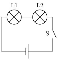
Figure 14: 串联电路
\begin{circuitikz}
  \draw (0,0) to[lamp, l=L1] (0,2)
  -- (1,2)
  to[nos, l=S] (3,2)
  -- (3,0)
  to[battery1](1,0)
  --(0,0);
  \draw (1.4,0) to[lamp,l=L2,*-*](1.4,2);

  \draw (6,0) -- (6,2)
  to[battery1] (9,2)
  -- (9,0)
  to[lamp, l=L2](7.5,0);
  \draw (6,0) to[nos, l=S2](7.5,0);
  \draw (6,1) to[nos, l=S1, *-](7.5,1)
  to[lamp,l=L1, -*](9,1);
\end{circuitikz}
另一种方式是把电路中的用电器并列地连接在电路中的两点之间,这种连接方式称为并联(parallel connection),按照这种方式连接起来的电路称为并联电路。
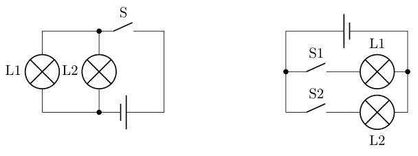
Figure 15: 并联电路
5. 电路图的难题
\begin{circuitikz}
  \draw (1.5,-0.4) node[below]{A};
  \draw (0,0) to[lamp,a=L1] (0,2)
  -- (3,2)
  to[lamp, a=L2] (3,0);
  \draw (0,0) to[nos, l=S] (3,0);

  \draw (5.5,-0.4) node[below]{B};
  \draw (4,0) to[battery1] (7,0)
  -- (7,2)
  to[lamp, a=L2] (5.5, 2)
  to[lamp, a=L1] (4, 2) -- (4, 0);
  \draw (4, 1) to[nos, a=S, *-] (5.5,1)
  to [short, -*](5.5,2);

  \draw (9.5,-0.4) node[below]{C};
  \draw (8,0) to[short] (11,0)
  to[lamp,a=L2](11,2) -- (8,2)
  to[lamp,a=L1](8,0);
  \draw (9,0) to[nos, a=S] (9,2);
  \draw (10,2) to[battery1](10,0);

  \draw (14.125,-0.4) node[below]{D};
  \draw (12.5,0) -- (15.5,0)
  to[lamp, l=L2] (15.5,2)
  -- (12.5,2) to[lamp, l=L1] (12.5,0);
  \draw (14,0) to[battery1,*-] (14,1)
  to[nos,l=S,-*](14,2);
\end{circuitikz}
在如图所示的各电路中,开关闭合后,小灯泡 L1、L2 都可能发光的是:
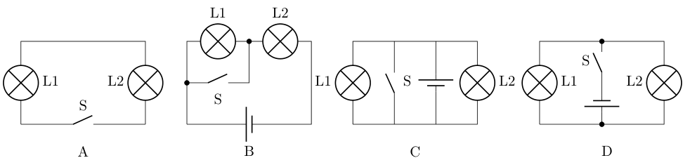
Figure 16: 电路图的难题
我把
- 题目
- 电路图
- circuitikz 源码
提交给费米分析。由于源码有助于对电路图的理解,费米很快得出正确答案 D,但费米对图 C 的分析有误:
逐图分析(开关 S 闭合后):
A 图——无电源,什么都不亮✗
B 图—— L1 被短路,只亮 L2 ✗
C 图—— L1 被短路,只亮 L2 ✗
D 图——两灯并联,都亮✓
因为图 C 电池都被短路了,应该 L1、L2 都不亮才对,而不是只亮 L2。
我只把
- 题目
- 电路图(不包括源码)
发给费米分析,费米背后的 deepseek-v4-flash 模型不是识图模型,自己不能识图,它就把电路图 PNG 文件通过 ask_expert 发给 DeepSeek 识图模式看:
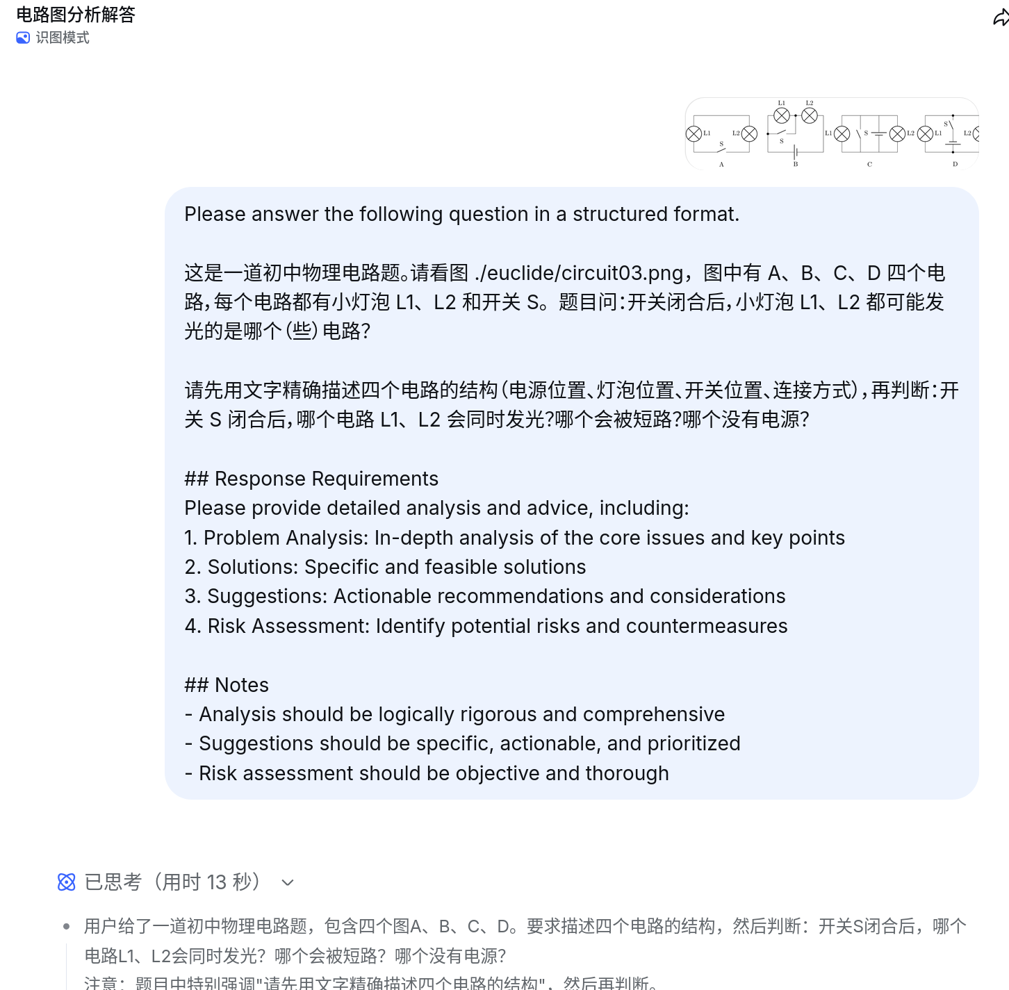
Figure 17: 识图模式识别电路图
识图模式给出答案:图 B 和图 D。 flash 得到识图模式的分析,虽然自己看不见但死活不相信这个答案,于是它再次追问:
Figure 18: 针对不明答案的追问
结果识图模式越描越黑。费米对识图模式终于绝望,于是开始自己分析。它先用程序读出图片尺寸(982×235),按坐标网格逐像素重建电路拓扑——59.1 像素对应 1 个单位,用 A/B/C/D 标签位置校准坐标,A 图中灯泡的位置与源码严格吻合,证明映射正确。然后逐图判定开关 S 闭合后的状态:
- A 图:只有 L1、L2、S 成环,没有电池,什么都不亮✗
- B 图:x=353(对应源码坐标 5.5)处有一根竖线从顶轨直通 y=1 的开关线,正是源码里
to [short, -*](5.5,2)的短接线;S 闭合后电流经短接线直接回电池负极,L1 被短路,只亮 L2 ✗ - C 图:L1、S、电池、L2 四根竖臂全部并联在上下轨之间,S 闭合等于导线短接电池正负极,电源短路,两灯都不亮✗
- D 图:电池和开关串联在中支路,L1、L2 分居两侧,S 闭合后两灯并联同时发光✓
最终花了 0.46 元排除迷惑项 B,得出正确答案 D。另外它对 C 的分析也是对的:
L1 和 L2 都不亮。
这次经历也说明, circuitikz 源码对 AI 分析电路图帮助巨大:没有源码时只能依赖识图模型,而小尺寸图片里开关、短接线只有几个像素,视觉模型很容易看错;有了源码,元件的坐标和连接关系都是精确的,任何会读代码的模型都能直接分析,不必去猜那几个像素。